Introduction to the CD4066
1. Overview
The CD4066 is a quad bilateral analog switch, mainly used for multiplexing analog or digital signals. Each CD4066 package contains 4 independent analog switches. Each switch has input, output, and control terminals; the input and output terminals are interchangeable.
 2. Pin Description
- CONTROL: switch control pin [1]
- IN/OUT: input/output pin
- OUT/IN: output/input pin
- VDD: positive supply
- VSS: negative supply
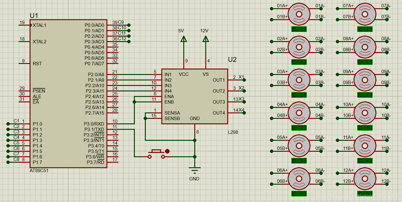
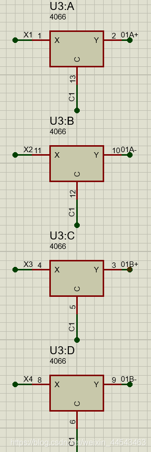
3. Control Method Connect the four inputs of the CD4066 to the L298N outputs and the CD4066 outputs to the stepper motor’s A+, A-, B+, and B- terminals. Tie all four control pins to one MCU pin so a single pin can switch all four switches on the CD4066 together, enabling stepper motor selection.
Proteus Simulation
The Proteus wiring diagram is shown below.
 Because Proteus does not include the CD4066—only the 4066—we treat a combination of 4 4066 chips as a single unit.
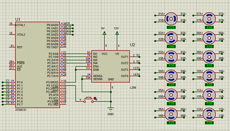
 Simulation results:
 Code:
Code:
#include<reg52.h>
sbit enable = P3^0;
sbit key = P3^1;
void delay(int i)
{
	int j;
	for(;i>0;i--)
		for(j=114;j>0;j--);
}

void main()
{
	unsigned char step[] = {0x01,0x02,0x04,0x08};	//顺时针转动
	//unsigned char istep[] = {0x01,0x02,0x04,0x08}; //逆时针转动
	unsigned char table1[] = {0x01,0x02,0x04,0x08,0x10,0x20,0x40,0x80};
	unsigned char table2[] = {0x01,0x02,0x04,0x08};
	int i=0,num=0;
	enable=1;
	P1 = 0x00;
	P0 = 0x00;
	while(1)
	{
		if(key == 0);
		{
			delay(10);
			if(key == 0)
			{
				num++;
				if(num>=12)
					num=-1;
				while(!key);
			}
		}

		if(num==-1)
		{
			P1=0x00;
			P0=0x00;
		}
		else if(num<8)
			P1=table1[num];
		else
			P0=table2[num-8];

		for(i=0; i<4; i++)
		{
			P2 = step[i];
			delay(500);
		}
	}
}
Comments